- 您现在的位置:买卖IC网 > Sheet目录518 > SQM110N04-03L-GE3 (Vishay Siliconix)MOSFET N-CH D-S 40V TO263
SQM110N04-03L
www.vishay.com
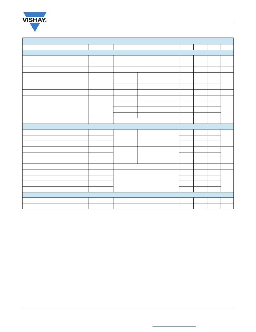
SPECIFICATIONS (T C = 25 °C, unless otherwise noted)
Vishay Siliconix
PARAMETER
SYMBOL
TEST CONDITIONS
MIN.
TYP.
MAX.
UNIT
Static
Drain-Source Breakdown Voltage
Gate-Source Threshold Voltage
Gate-Source Leakage
V DS
V GS(th)
I GSS
V GS = 0, I D = 250 μA
V DS = V GS , I D = 250 μA
V DS = 0 V, V GS = ± 20 V
V GS = 0 V
V DS = 40 V
40
1.5
-
-
-
2.0
-
-
-
2.5
± 100
1.0
V
nA
Zero Gate Voltage Drain Current
I DSS
V GS = 0 V
V DS = 40 V, T J = 125 °C
-
-
50
μA
V GS = 0 V
V DS = 40 V, T J = 175 °C
-
-
250
On-State Drain Current a
I D(on)
V GS = 10 V
V DS ??? 5 V
120
-
-
A
V GS = 10 V
I D = 30 A
-
0.0027
0.0035
Drain-Source On-State Resistance a
R DS(on)
V GS = 10 V
V GS = 10 V
I D = 30 A, T J = 125 °C
I D = 30 A, T J = 175 °C
-
-
-
-
0.0057
0.0070
?
V GS = 4.5 V
I D = 20 A
-
0.0041
0.0053
Forward Transconductance b
g fs
V DS = 15 V, I D = 30 A
-
106
-
S
Dynamic b
Input Capacitance
C iss
-
4252
5315
Output Capacitance
C oss
V GS = 0 V
V DS = 25 V, f = 1 MHz
-
854
1070
pF
Reverse Transfer Capacitance
Total Gate Charge c
C rss
Q g
-
-
472
93
590
140
Gate-Source Charge c
Q gs
V GS = 10 V
V DS = 20 V, I D = 110 A
-
14.6
-
nC
Gate-Drain Charge c
Q gd
-
19.2
-
Gate Resistance
Time c
Turn-On Delay
Rise Time c
Turn-Off Delay Time c
Fall Time c
R g
t d(on)
t r
t d(off)
t f
f = 1 MHz
V DD = 20 V, R L = 0.18 ?
I D ? 110 A, V GEN = 10 V, R g = 1 ?
0.5
-
-
-
-
1.1
15
13
52
16
1.7
23
20
78
24
?
ns
Source-Drain Diode Ratings and Characteristics b
Pulsed Current a
I SM
-
-
480
A
Forward Voltage
V SD
I F = 100 A, V GS = 0
-
0.9
1.5
V
Notes
a. Pulse test; pulse width ? 300 μs, duty cycle ? 2 %.
b. Guaranteed by design, not subject to production testing.
c. Independent of operating temperature.
Stresses beyond those listed under “Absolute Maximum Ratings” may cause permanent damage to the device. These are stress ratings only, and functional operation
of the device at these or any other conditions beyond those indicated in the operational sections of the specifications is not implied. Exposure to absolute maximum
rating conditions for extended periods may affect device reliability.
S11-2035-Rev. C, 17-Oct-11
2
Document Number: 64719
THIS DOCUMENT IS SUBJECT TO CHANGE WITHOUT NOTICE. THE PRODUCTS DESCRIBED HEREIN AND THIS DOCUMENT
ARE SUBJECT TO SPECIFIC DISCLAIMERS, SET FORTH AT www.vishay.com/doc?91000
发布紧急采购,3分钟左右您将得到回复。
相关PDF资料
SQM110N06-04L-GE3
MOSFET N-CH D-S 60V TO263
SQM40N10-30-GE3
MOSFET N-CH D-S 100V TO263
SQM85N03-06P-GE3
MOSFET N-CH D-S 30V TO263
SQR50N03-06P-GE3
MOSFET N-CH D-S 30V TO263
SQS400EN-T1-GE3
MOSFET N-CH 40V 16A TO263
SQS401EN-T1-GE3
MOSFET P-CH D-S 40V PPAK 1212-8
SSA-LXB102GD
LED ARRAY 3MM 10SEG FLAT TOP GRN
SSA-LXB102ID
LED ARRAY 3MM 10SEG FLAT TOP RED
相关代理商/技术参数
SQM110N04-04-GE3
功能描述:MOSFET 40V 120A 250W 3.5mohm @ 10V RoHS:否 制造商:STMicroelectronics 晶体管极性:N-Channel 汲极/源极击穿电压:650 V 闸/源击穿电压:25 V 漏极连续电流:130 A 电阻汲极/源极 RDS(导通):0.014 Ohms 配置:Single 最大工作温度: 安装风格:Through Hole 封装 / 箱体:Max247 封装:Tube
SQM110N05-06L-GE3
功能描述:MOSFET 55V 110A 158W 6.0mohm @ 10V
RoHS:否 制造商:STMicroelectronics 晶体管极性:N-Channel 汲极/源极击穿电压:650 V 闸/源击穿电压:25 V 漏极连续电流:130 A 电阻汲极/源极 RDS(导通):0.014 Ohms 配置:Single 最大工作温度: 安装风格:Through Hole 封装 / 箱体:Max247 封装:Tube
SQM110N06-04L-GE3
功能描述:MOSFET 60V 120A 437.5W 3.5mohm @ 10V RoHS:否 制造商:STMicroelectronics 晶体管极性:N-Channel 汲极/源极击穿电压:650 V 闸/源击穿电压:25 V 漏极连续电流:130 A 电阻汲极/源极 RDS(导通):0.014 Ohms 配置:Single 最大工作温度: 安装风格:Through Hole 封装 / 箱体:Max247 封装:Tube
SQM110N06-06-GE3
功能描述:MOSFET 60V 120A 230W 6.0mohm @ 10V RoHS:否 制造商:STMicroelectronics 晶体管极性:N-Channel 汲极/源极击穿电压:650 V 闸/源击穿电压:25 V 漏极连续电流:130 A 电阻汲极/源极 RDS(导通):0.014 Ohms 配置:Single 最大工作温度: 安装风格:Through Hole 封装 / 箱体:Max247 封装:Tube
SQM110N08-05-GE3
功能描述:MOSFET N-CH D-S 75V TO263 RoHS:是 类别:分离式半导体产品 >> FET - 单 系列:TrenchFET® 标准包装:1,000 系列:MESH OVERLAY™ FET 型:MOSFET N 通道,金属氧化物 FET 特点:逻辑电平门 漏极至源极电压(Vdss):200V 电流 - 连续漏极(Id) @ 25° C:18A 开态Rds(最大)@ Id, Vgs @ 25° C:180 毫欧 @ 9A,10V Id 时的 Vgs(th)(最大):4V @ 250µA 闸电荷(Qg) @ Vgs:72nC @ 10V 输入电容 (Ciss) @ Vds:1560pF @ 25V 功率 - 最大:40W 安装类型:通孔 封装/外壳:TO-220-3 整包 供应商设备封装:TO-220FP 包装:管件
SQM110N10-09-GE3
功能描述:MOSFET N-CH D-S 100V TO263 RoHS:是 类别:分离式半导体产品 >> FET - 单 系列:TrenchFET® 标准包装:1,000 系列:MESH OVERLAY™ FET 型:MOSFET N 通道,金属氧化物 FET 特点:逻辑电平门 漏极至源极电压(Vdss):200V 电流 - 连续漏极(Id) @ 25° C:18A 开态Rds(最大)@ Id, Vgs @ 25° C:180 毫欧 @ 9A,10V Id 时的 Vgs(th)(最大):4V @ 250µA 闸电荷(Qg) @ Vgs:72nC @ 10V 输入电容 (Ciss) @ Vds:1560pF @ 25V 功率 - 最大:40W 安装类型:通孔 封装/外壳:TO-220-3 整包 供应商设备封装:TO-220FP 包装:管件
SQM110P04-04L-GE3
功能描述:MOSFET P-CH 40V 120A TO263 RoHS:是 类别:分离式半导体产品 >> FET - 单 系列:TrenchFET® 标准包装:1,000 系列:MESH OVERLAY™ FET 型:MOSFET N 通道,金属氧化物 FET 特点:逻辑电平门 漏极至源极电压(Vdss):200V 电流 - 连续漏极(Id) @ 25° C:18A 开态Rds(最大)@ Id, Vgs @ 25° C:180 毫欧 @ 9A,10V Id 时的 Vgs(th)(最大):4V @ 250µA 闸电荷(Qg) @ Vgs:72nC @ 10V 输入电容 (Ciss) @ Vds:1560pF @ 25V 功率 - 最大:40W 安装类型:通孔 封装/外壳:TO-220-3 整包 供应商设备封装:TO-220FP 包装:管件
SQM110P06-07L-GE3
功能描述:MOSFET P-CH 60V 120A TO263 RoHS:是 类别:分离式半导体产品 >> FET - 单 系列:TrenchFET® 标准包装:1,000 系列:MESH OVERLAY™ FET 型:MOSFET N 通道,金属氧化物 FET 特点:逻辑电平门 漏极至源极电压(Vdss):200V 电流 - 连续漏极(Id) @ 25° C:18A 开态Rds(最大)@ Id, Vgs @ 25° C:180 毫欧 @ 9A,10V Id 时的 Vgs(th)(最大):4V @ 250µA 闸电荷(Qg) @ Vgs:72nC @ 10V 输入电容 (Ciss) @ Vds:1560pF @ 25V 功率 - 最大:40W 安装类型:通孔 封装/外壳:TO-220-3 整包 供应商设备封装:TO-220FP 包装:管件
